20 Mar
graphics card


Nvidia has unveiled its latest AI chip called Blackwell, which is 30 times faster at certain tasks than its predecessor. The company, which sits with a market share of 80%, hopes to cement its dominance in the market. In addition to the B200 "Blackwell" chip, company CEO Jensen Huang detailed a new set of software tools at the company's annual developer conference.
Named after Dr. David Harold Blackwell, an American pioneer in statistics and mathematics who, among other things, wrote the first Bayesian statistics textbook, the Blackwell architecture is once again NVIDIA betting big on many of the company's AI designs. NVIDIA has something really good going with the Hopper (and Ampere before it), and overall Blackwell aims to bring more of the same, but with more features, more flexibility and more transistors.
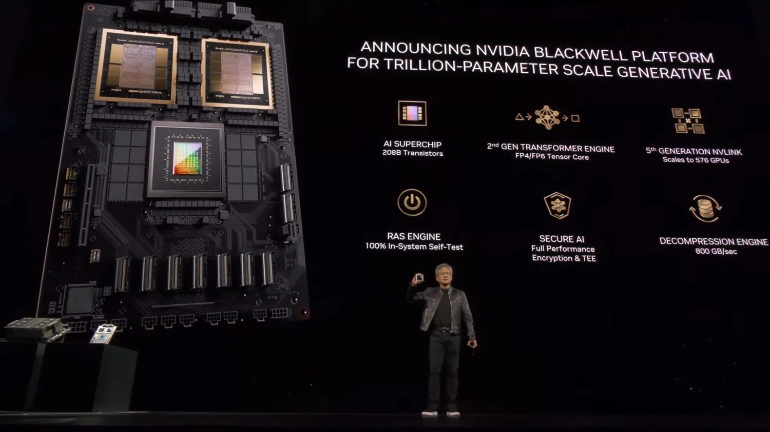
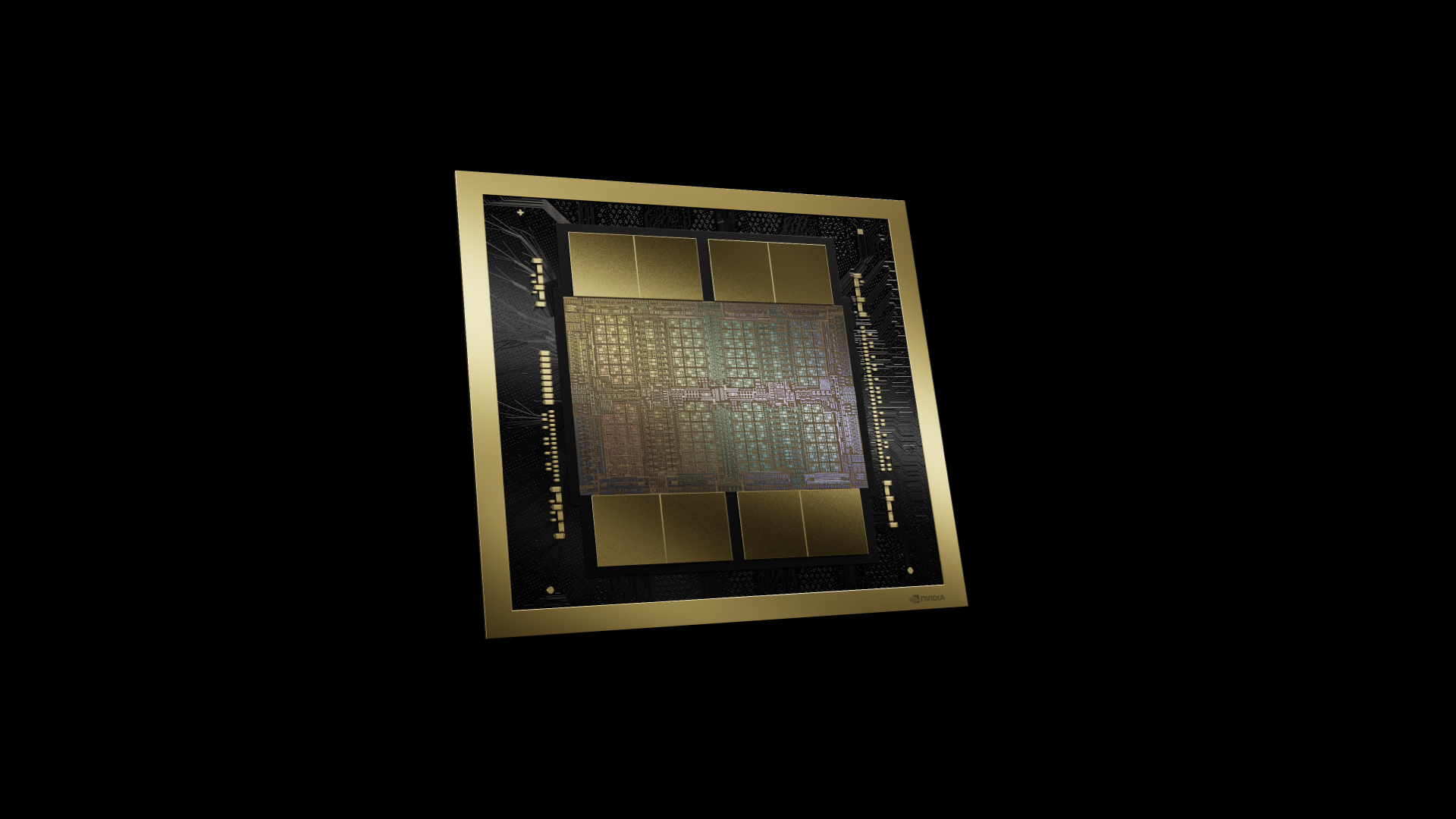
The first thing to note is that the Blackwell GPU is going to be big. Literally. The B200 modules it will go into will have two GPU dies on a single package. NVIDIA has finally moved to chiplet designs with their flagship GPUs. While they don't reveal the size of the individual dies, we're told they're "reticle-sized" dies, which should put them somewhere over 800mm2 each. The GH100 die was already close to TSMC's 4nm reticle limits, so there's very little room for NVIDIA to grow here - at least without staying within a single die.
Curiously, despite these die space limitations, NVIDIA is not using a TSMC 3nm-class node for the Blackwell. Technically, they're using a new node - the TSMC 4NP - but this is just a high-performance version of the 4N node that was used for the GH100 GPU. This means that virtually all of Blackwell's efficiency gains must come from architectural efficiency, while a mix of that efficiency and the size of scaling out will deliver Blackwell's overall performance improvements.
Despite sticking to a 4nm-class node, NVIDIA has managed to squeeze more transistors into a single die. The transistor count for the complete accelerator is 208 billion, or 104 billion transistors per die. The GH100 was 80 billion transistors, so each B100 die has about 30% more transistors overall, a modest gain compared to historical standards. Which in turn is why we see NVIDIA applying more dies to their complete GPU.
For their first multi-die chip, NVIDIA is determined to skip the awkward "two accelerators on one chip" phase and go straight to making the entire accelerator behave as a single chip. According to NVIDIA, the two dies act as "a unified CUDA GPU," offering full performance without compromise. Key to this is the high-bandwidth I/O connection between dies, which NVIDIA calls the NV-High Bandwidth Interface (NV-HBI), offering 10TB/second of bandwidth. Presumably it's in aggregated form, meaning the dies can send 5TB/second in each direction simultaneously.
On the B200, each die is paired with 4 stacks of HBM3E memory, for a total of 8 stacks in total, forming an effective memory bus width of 8192-bits. One of the limiting factors in all AI accelerators has been memory capacity (not to underestimate the need for bandwidth as well), so being able to include more stacks is huge in improving the local memory capacity of the accelerator. Overall, the B200 offers 192 GB of HBM3E, or 24 GB per stack, which is identical to the capacity of 24 GB per stack for the H200 (and 50% more memory than the original 16 GB per stack H100).
According to NVIDIA, the chip has a total HBM memory bandwidth of 8TB/second, which equates to 1TB/second per stack – or a data rate of 8Gbps/pin. As we noted in our previous coverage of the HBM3E, the memory is ultimately designed to reach 9.2Gbps/pin or better, but we often see NVIDIA being a bit conservative with the clock speeds of their server accelerators. Either way, this is almost 2.4 times as much memory bandwidth as the H100 (or 66% more than the H200), so NVIDIA is seeing a significant increase in bandwidth.
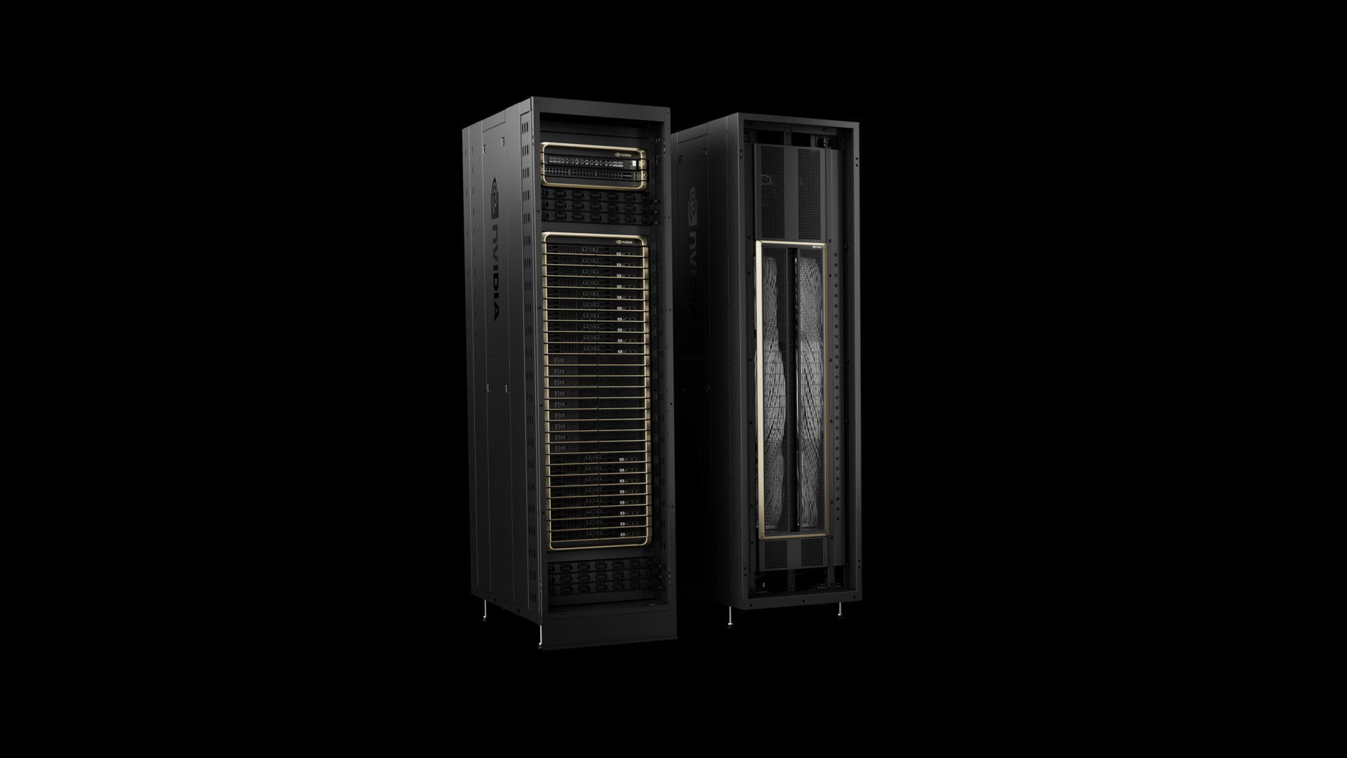
Finally, we currently have no information on the TDP of a single B200 accelerator. Undoubtedly it will be high - you can't more than double your transistors in one and avoid some kind of penalty in terms of power consumption. NVIDIA will sell both air-cooled DGX systems and liquid-cooled NVL72 racks, so the B200 is not out of air cooling's reach.
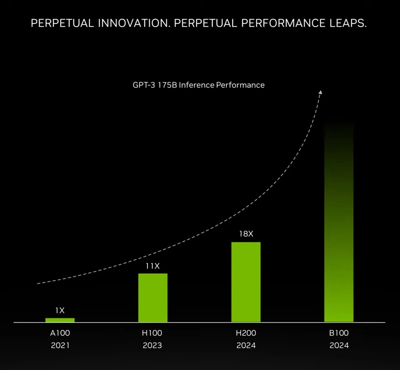
Overall, NVIDIA is targeting a 4x increase in training performance over the H100 at the cluster level, and an even greater 30x increase in inference performance, while doing so with 25x greater energy efficiency.
Nvidia is the third most valuable company in the US, surpassed only by Microsoft and Apple. Its shares have risen 240% in the past year and its market capitalization reached $2tn last month.
As Mr. Huang kicked off the conference, he jokingly said, "I hope you realize that this is not a concert." Nvidia said major customers such as Amazon, Google, Microsoft and OpenAI are expected to use the company's new flagship chip in cloud-computing services and for their own AI offerings. It also said the new software tools, called micro-services, improve system efficiency and make it easier for a company to integrate an AI model into its work.
Other announcements include a new line of chips for cars that can run chatbots inside the vehicle. The firm said Chinese electric car makers BYD and Xpeng would both use its new chips. Sir. Huang also outlined a new series of chips for creating humanoid robots and invited several of the robots up on stage with him.