AMD Ryzen 3000 and X570 Explained
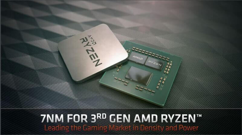
The Zen 2 Architecture
Zen 2 is in fact AMD’s third generation of Ryzen processors, and along with the new X570 chipset, a multitude of noteworthy upgrades comes with it. As such, we’d like to introduce you to some of the more important aspects and explain the fundamentals of these.
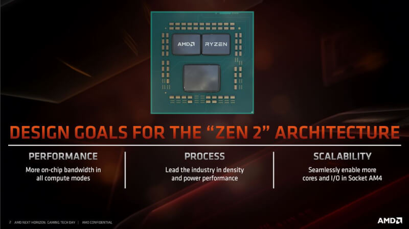
In general terms, it’s all about bringing even more bandwidth into the new line-up of consumer-targeted processors. The purpose is to bring more cores, and thereby more power to workstation tasks, without compromising with affordable prices. Zen 2, which is also known as Ryzen 3000, is built on the 7 nm chip die similar to that of our previously tested AMD Radeon VII graphics card. This is a 42% smaller surface area on the new chips, which makes room for more cores and less heat buildup.
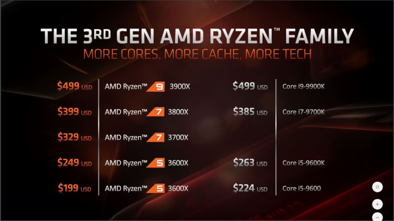
The new Ryzen series starts at an MSRP of $199 for the Ryzen 5 3600X and runs all the way up to $499 for the Ryzen 9 3900X. The prices are a good match for Intel’s 9th generation Core processors. Exactly how well they are performing in comparison to Intel you can read in our recent product reviews.
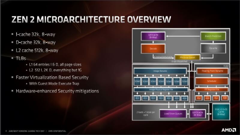
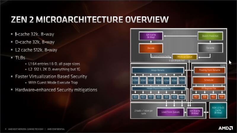
Here, we see an overview of how the new Ryzen processors are built in terms of cache, threads per core and integer units. All cores are built with its own L1 and L2 cache, and they share a larger L3 cache.
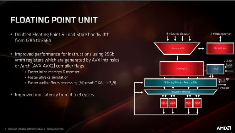
AMD has increased the number of Floating Point Units (FPUs) from 128 b to 256 b, which makes the new processors capable of handling more instructions at a time.
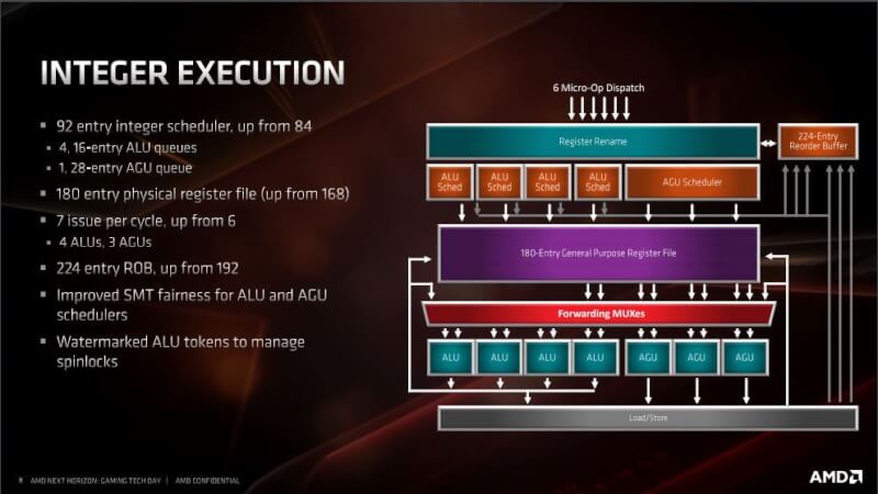
Zen 2 manages to squeeze 32 extra ROBs into the new CPUs. An ROB is a buffer that is used to send instructions from the CPU into the appropriate registers or merely to the memory so they are ready to be used. The high internal bandwidth has created a demand for a larger buffer and that’s exactly what we get. In general, AMD has increased the bandwidth of Zen 2 across the board, and on paper it should give us a reasonable performance gain.
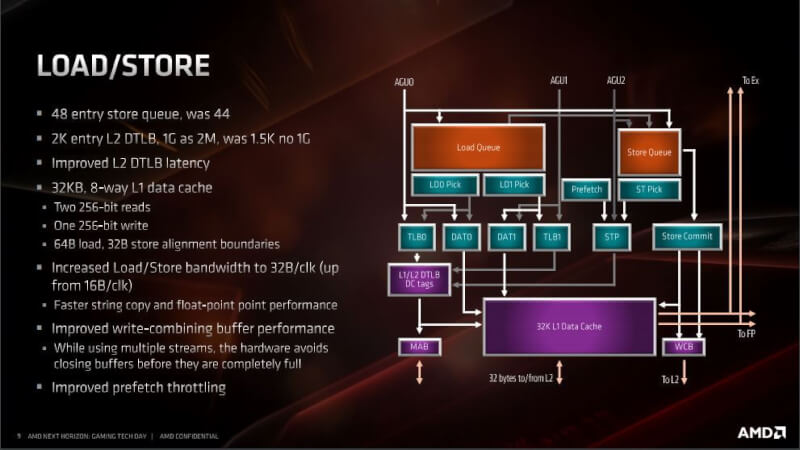
The Load/Store bandwidth has also been doubled. This is the amount of instructions that can be handled simultaneously. These instructions are data that is loaded in and out of the memory or the processor’s registers. By increasing the Load/Store Units, AMD has made Zen 2 ready for the higher bandwidth. So, it seems that there is a good connection between these improvements. But it will be down to benchmarking tests to see if this actually pays off in the end.
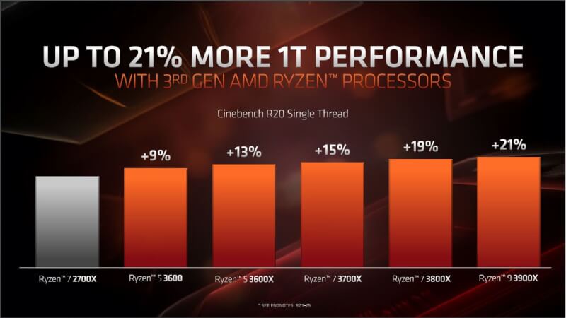
All of these improvements should manifest themselves in the form of performance gains, and according to AMD’s own comparison to the Ryzen 7 2700X it would certainly seem that we get more performance per core. At least that’s what their single core Cinebench R20 test shows.
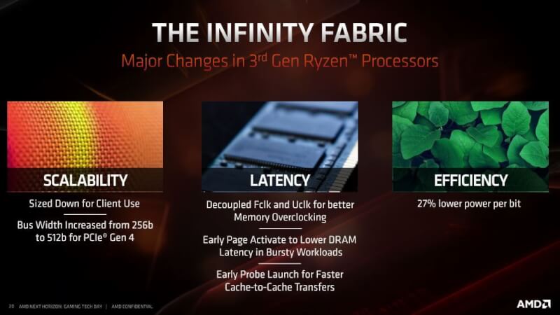
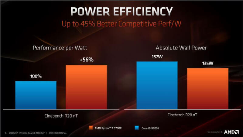
One of the significant improvements in AMD’s Infinity Fabric die is the increase on the bus from 256 bit to 512 bit, which is an advantage in correlation with the new PCIe Gen. 4 technology. Also, the memory controller has been optimized and together with the smaller 7 nm chip die the overall energy efficiency has been optimized by 27%.
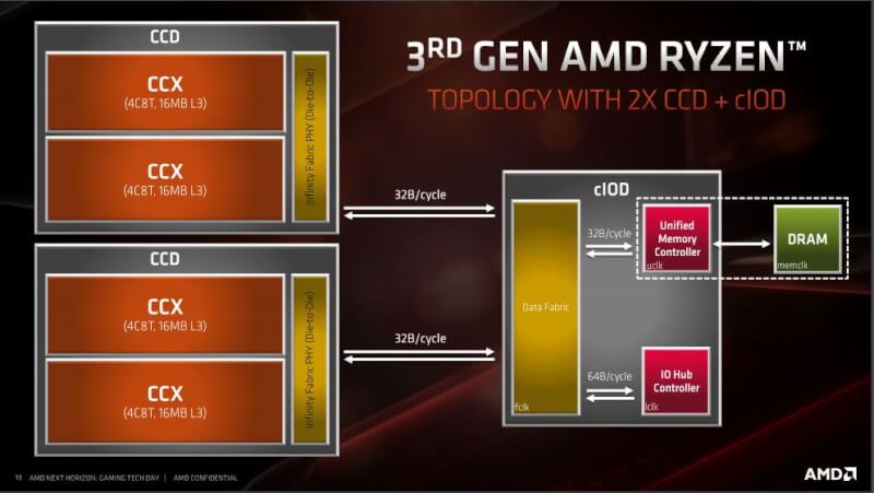
With their Zen architecture, AMD has split their cores up in multiple CCX’s. A CCX is a cluster of four Zen cores that are connected by a shared L3 cache. In the new Zen 2 processors, two CCX’s can cooperate in a CCD which then consists of two times four cores that play together via a cIOD and an L3 cache. The purpose of this design is that the workload is fed to the core one at a time, until it reaches its limit of instructions per second, after which the next core takes over. This continues until the entire processor is in use. No core boosts to its maximum frequency if there’s nothing for them to do.
The AMD X570 Chipset
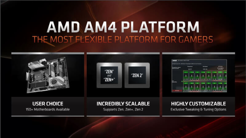
It’s time to talk a bit about the X570 chipset and what it brings to the table. We already know that there are over 150 different motherboard within this series, and we still have yet to see many of these in real-life.
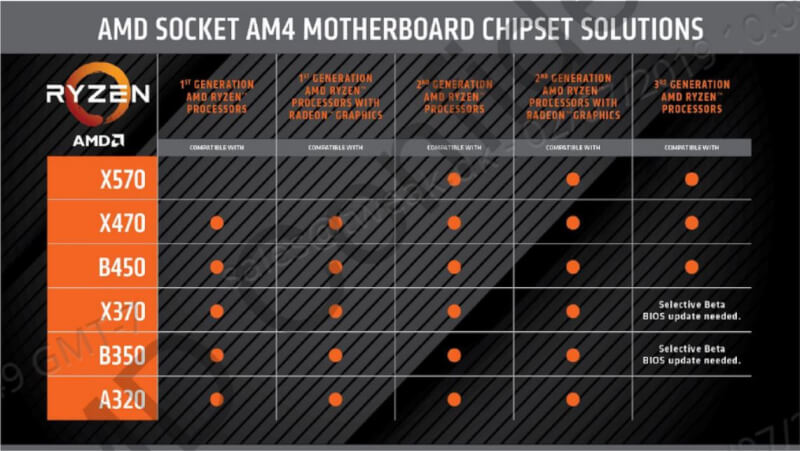
The Zen 2 processors are actually backwards compatible with several different chipsets. Many of these, in fact, straight out of the box, and others with a BIOS update, which should follow closely with the release of Ryzen 3000. Similarly, the Zen and Zen+ processors are compatible with X570. There will, of course, be some functionality of the Zen 2 that will not work on X470 and under, just like Zen and Zen+ won’t be able to take advantage of all of the functionality of the X570. In general, there’s a lot of flexibility here, for instance if you already have a relatively new X470 motherboard, but want to upgrade to a Zen 2 processor.
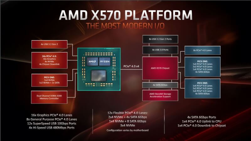
The new Zen 2 Ryzen 3000 processors come with four USB 3.2 lanes and 24 PCIe Gen. 4 lanes, of which 16 are reserved for the graphics card, four for the NVMe and four for the chipset downlink. In addition, there are lanes for either one x4 NVMe or an x2 NVMe , two SATA6 drives and a dual channel 3200 MHz DDR4 controller. All in all, we get 20/24 PCIe Gen. 4 lanes.
The X570 chipset comes with eight PCIe Gen. 4 lanes and, in addition, four lanes more for either an x4 NVMe, two x2 NVMe or four SATA6 drives plus an x4 PCIe Gen. 4 uplink to the CPU. In total, the chipset has 20 PCIe Gen. 4 lanes. Aside from that, it is still possible for the motherboard manufacturers to add, for instance, external SATA controllers, which makes it possible to allocate some of the many SATA lanes to for example graphics card solutions.
Latest motherboard
-
26 Sepmotherboard
-
04 Febmotherboard
ASRock X870 Steel Legend WiFi
-
09 Janmotherboard
ASUS ROG Strix X870-I Gaming WiFi
-
02 Decmotherboard
ASRock Phantom Gaming X870E Nova WiFi
-
28 Novmotherboard
ASUS TUF Gaming X870-Plus WiFi
-
28 Novmotherboard
ASRock Z890 Steel Legend WiFi
-
15 Novmotherboard
Gigabyte Z890 Aorus Elite Wifi7
-
11 Novmotherboard
ASRock Z890 Taichi
Most read motherboard
Latest motherboard
-
26 Sepmotherboard
MSI MPG Z890 CARBON WIFI
-
04 Febmotherboard
ASRock X870 Steel Legend WiFi
-
09 Janmotherboard
ASUS ROG Strix X870-I Gaming WiFi
-
02 Decmotherboard
ASRock Phantom Gaming X870E Nova WiFi
-
28 Novmotherboard
ASUS TUF Gaming X870-Plus WiFi
-
28 Novmotherboard
ASRock Z890 Steel Legend WiFi
-
15 Novmotherboard
Gigabyte Z890 Aorus Elite Wifi7
-
11 Novmotherboard
ASRock Z890 Taichi


