31 Mar
processor - cpu


According to the latest reports, Samsung Foundry will use its new SF2 (2nm-class) manufacturing process as the first with a backside power delivery (BSPDN). Chosun.com reports that the promising results achieved using backside power delivery have changed Samsung's view of the technology. This has led the company to consider the use of BSPDN in a commercial process.
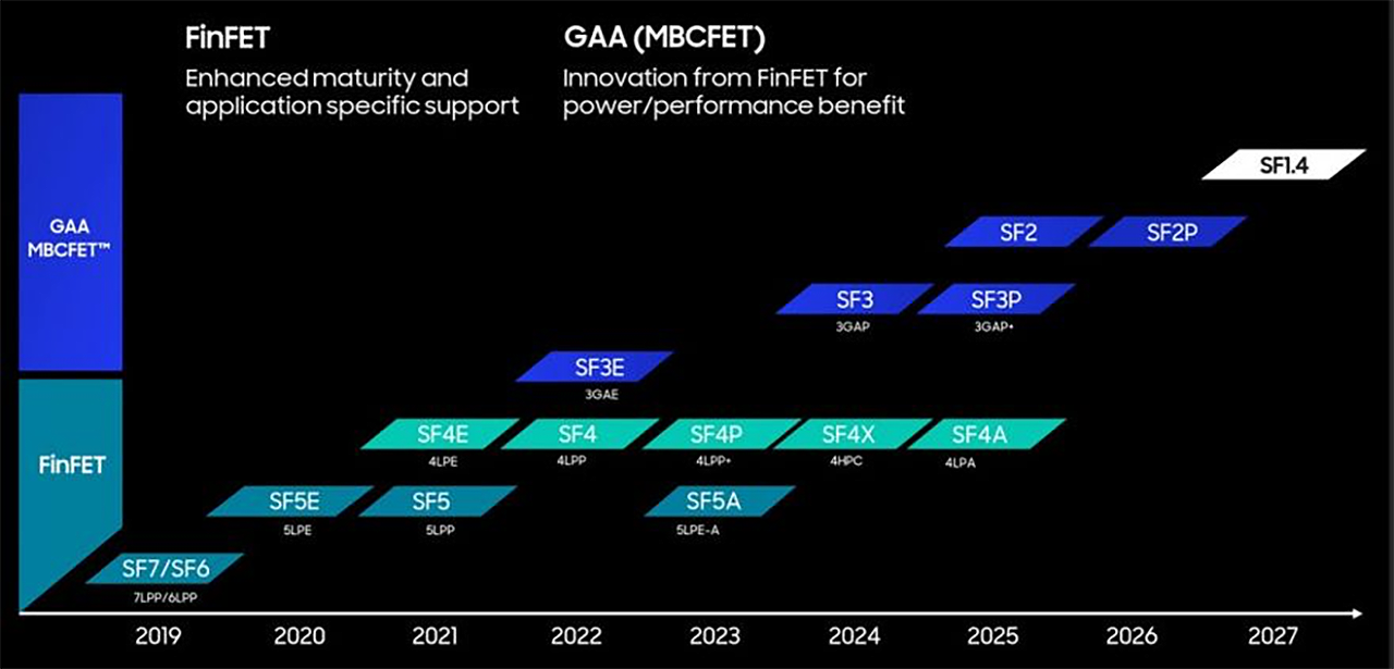
It was expected that Samsung would introduce backside power delivery with its 1.7nm-class fabrication node, but it will instead come with the SF2 process node in 2025. As Tom's Hardware points out, there are no 1.7nm-class nodes on Samsung's current roadmap. We can only see SF2, SF2P and SF1.4 process nodes.
Samsung has used two test chips based on Arm architecture with backside power delivery and achieved a reduction in the range of 10% and 19% without telling the world which process node was used.
Backside power delivery allows thicker, lower resistance wires, which are able to deliver more power, and thus more performance, with less power consumption. Samsung's research paper showed that backside power delivery has benefits such as a 3.6% increase in Fmax, a 2.4% reduction in standard block area, and a 1.6% improvement in standard block performance.
It appears that Samsung's decision to include backside power delivery in the upcoming SF2 process technology is a response to Intel's progress with its Intel 20A and Intel 18A production technologies coming in 2025, and TSMC's upcoming N2P process rolling off the production lines in 2026-2027.